
1. Introduction
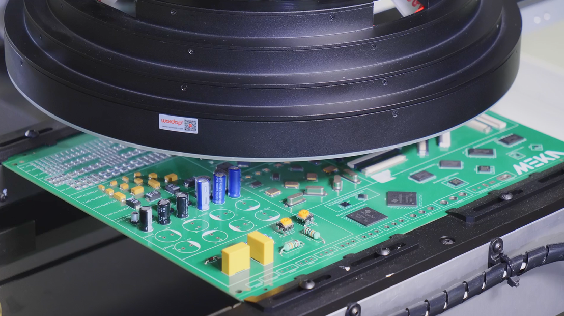
Automated Optical Inspection (AOI) is a high-precision detection system designed for the electronics manufacturing industry. It is primarily used to identify appearance defects, functional abnormalities, positional deviations, and soldering issues on printed circuit boards (PCBs). Key functions include:
Appearance Inspection: Verifies component size, shape, and color.
Functionality Check: Evaluates electrical connections and component layout.
Accuracy Assessment: Detects deviations in position, shape, and dimensions.
Fault Detection: Identifies common issues such as short circuits, open circuits, and cold solder joints.
AOI is capable of detecting excessive solder, insufficient solder, solder balls, and other soldering defects, making it ideal for high-precision, high-density applications such as smartphones and wearable devices.
2. Current Development
1. Technological Advancements
Progress in image processing, AI, and deep learning has significantly improved detection accuracy and speed.
2. Expanding Market Demand
As electronic products become more complex, the need for high reliability and quality continues to grow, driving AOI adoption in smartphones, automotive electronics, and medical devices.
3. Smart Integration
AOI is increasingly integrated with SPI and reflow soldering systems to form closed-loop automated lines, enhancing overall efficiency and yield.
4. Improved Usability
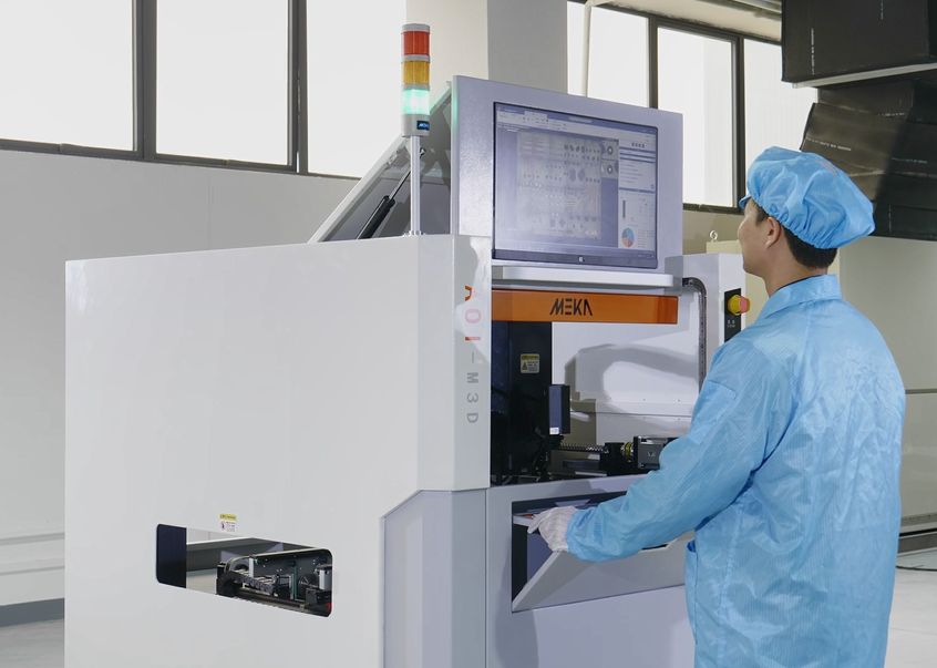
Modern AOI systems feature more intuitive interfaces and simplified setup processes, reducing the training threshold for operators.
5. Green Manufacturing
Energy-efficient design and optimized material usage align with sustainability and environmental goals.
3. Challenges
Intensifying market competition and rising demands for flexible, cost-effective solutions present ongoing challenges for AOI manufacturers.
4. Conclusion
AOI technology is evolving rapidly. To remain competitive, continuous innovation in detection performance and system integration is essential.