
In the electronics manufacturing industry, ensuring the quality and reliability of products is paramount. Automated Optical Inspection (AOI) has become a cornerstone technology for achieving this, with 2D AOI and 3D AOI being the most prominent approaches. While they share the same goal of detecting defects and ensuring production quality, their underlying technologies, capabilities, and applications vary greatly. This blog explores the differences, strengths, and ideal applications of these two AOI technologies in detail.
Understanding 2D AOI: Efficient and Cost-Effective
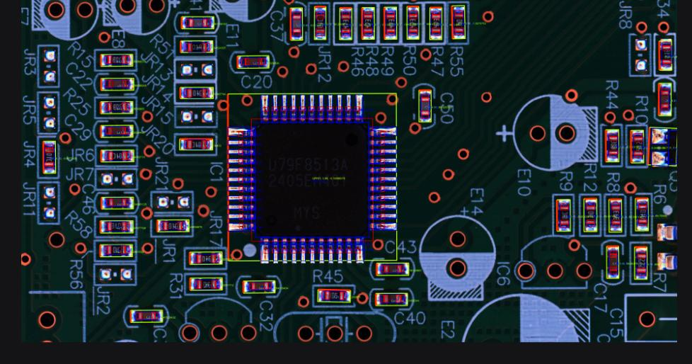
2D AOI uses a combination of cameras and lighting systems to capture high-resolution, flat (2D) images of printed circuit boards (PCBs). By analyzing features such as color, contrast, and shape, it identifies potential defects in solder joints, missing components, or misalignments.
Key Features of 2D AOI
Detection Mechanism: Operates purely on flat image data to identify issues on the board’s surface.
Strengths:
Cost-Effective: The technology is affordable, making it ideal for manufacturers with limited budgets.
Fast Throughput: Its rapid image-capture process is suitable for high-volume production lines where speed is critical.
Proven Technology: 2D AOI has been in use for many years, ensuring stability and reliability in simpler applications.
Limitations:
Lack of Height Measurement: 2D AOI cannot detect defects that involve height or volume, such as solder paste thickness or insufficient solder joints.
Lighting Sensitivity: Changes in light conditions can lead to false positives or missed defects.
Challenging Complex Boards: As PCBs become more densely packed with smaller components, 2D AOI struggles to provide the precision needed.
When to Use 2D AOI
2D AOI is perfect for:
Simple PCB designs.
Mass production where speed outweighs precision.
Low-to-mid complexity applications where defects are surface-based.
Exploring 3D AOI: Precision and Versatility
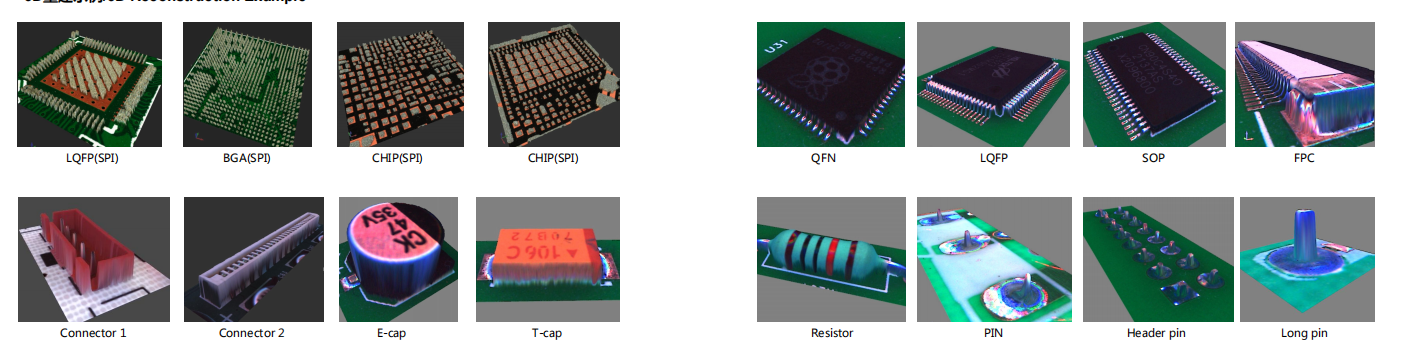
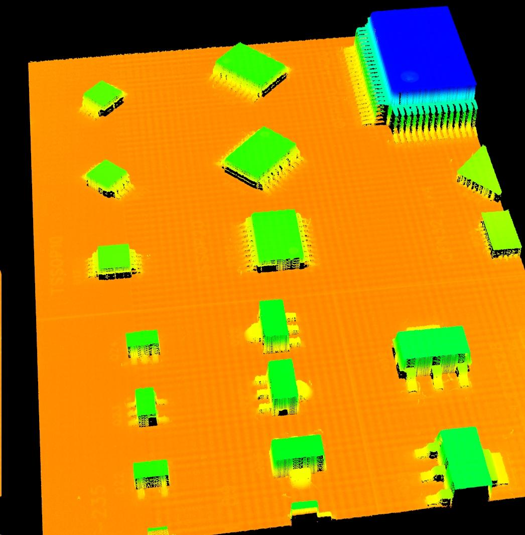
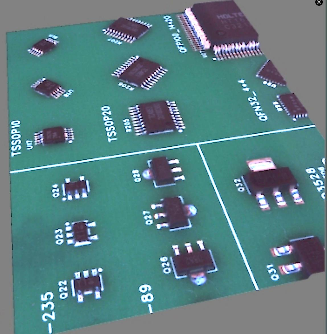
3D AOI goes a step further by incorporating three-dimensional data into its inspections. Using technologies such as structured light projection, laser triangulation, or fringe projection, 3D AOI captures height and volume information alongside 2D imagery. This enables it to create detailed 3D models of PCBs, allowing for more accurate and comprehensive inspections.
Key Features of 3D AOI
Detection Mechanism: Combines 2D imaging with depth data, measuring component height, solder volume, and other critical parameters.
Strengths:
Exceptional Precision: 3D AOI excels at detecting defects like insufficient solder, tombstoning (components standing upright), and coplanarity issues.
Adaptability: It performs well with high-density boards, miniature components, and complex assemblies.
Robustness: Less dependent on lighting conditions, reducing false positives and improving reliability.
Future-Proof: As components get smaller and PCB designs more complex, 3D AOI is better equipped to meet future challenges.
Limitations:
Higher Costs: The initial investment is significant due to the advanced hardware and software.
Slower Speed: While still efficient, 3D AOI inspections can take longer than 2D AOI, particularly for intricate boards.
When to Use 3D AOI
3D AOI is ideal for:
Complex PCBs with high-density components.
Products requiring strict quality standards, such as automotive electronics, aerospace, and medical devices.
Applications where height, volume, or coplanarity are critical factors.
Comparative Overview: 2D AOI vs. 3D AOI
| Aspect | 2D AOI | 3D AOI |
|---|---|---|
| Technology | 2D imaging | 2D + 3D imaging |
| Precision | Limited; no height or volume detection | High; includes height, volume, and coplanarity |
| Speed | Faster for simple inspections | Slightly slower but more comprehensive |
| Cost | Lower upfront cost | Higher investment |
| Lighting Dependency | High; prone to false positives | Low; stable under varied lighting |
| Application | Simple or standard PCBs | High-density, high-complexity PCBs |
Making the Right Choice for Your Production Line
Choosing between 2D and 3D AOI depends on several factors:
1. Budget and Scale
If cost is a primary concern and your production involves standard PCBs with minimal complexity, 2D AOI is the logical choice.
2. Complexity and Quality Standards
For high-value products or those requiring exceptional reliability (e.g., automotive, aerospace, or medical), 3D AOI provides unparalleled precision and insight.
3. Production Environment
In mixed production environments, consider combining both systems:
Use 2D AOI for quick inspections and high-speed defect filtering.
Deploy 3D AOI for detailed analysis of critical areas or complex boards.
Future Trends in AOI Technology
As the electronics industry evolves, AOI systems are becoming smarter and more integrated. Features such as AI-powered defect recognition, real-time analytics, and enhanced adaptability are now being incorporated into both 2D and 3D AOI systems. This evolution ensures manufacturers can keep up with increasing quality demands and rapidly changing PCB designs.
Conclusion
Both 2D and 3D AOI have their distinct roles in the manufacturing process. While 2D AOI remains a cost-effective solution for simpler tasks, 3D AOI is rapidly becoming the go-to choice for precision-critical applications. Understanding your specific production needs will help you make an informed decision, maximizing efficiency, quality, and value.
Have questions about AOI technology or want to explore how it can improve your manufacturing process? Drop a comment below, and let’s discuss how to optimize your inspection strategy!